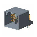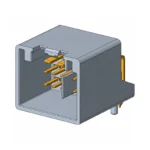


When a hardware lead in Austin reduced a controller enclosure by moving a header closer to the wall in an illustrative design-review scenario, the prototype powered up, but the harness could no longer be removed without bending the board. The connector met its catalog dimensions; the layout had ignored the mating path and technician’s grip clearance. The apparent component problem was actually a board-and-enclosure integration decision.
Summary: Choose a pin connector by treating the header, mating housing, contacts, PCB footprint and assembly process as one controlled system. Pin count sets circuit capacity, while pitch sets only contact spacing; neither establishes current, voltage, retention or durability. Before sourcing, lock the mating direction, keep-outs, electrical loading, wire termination, environmental tests and revision-controlled drawings. Prototype the complete connection—not just the header.
Choose the connector architecture before comparing pitch
A pin connector can be an open header, a shrouded and keyed assembly, a right-angle edge interface or a surface-mount part with board-retention features. The right choice depends on who mates it, how often, and whether the surrounding assembly prevents offset or reversed insertion. The site’s Pin Header guide adds useful selection context, but only the proposed supplier drawing defines the actual interface.
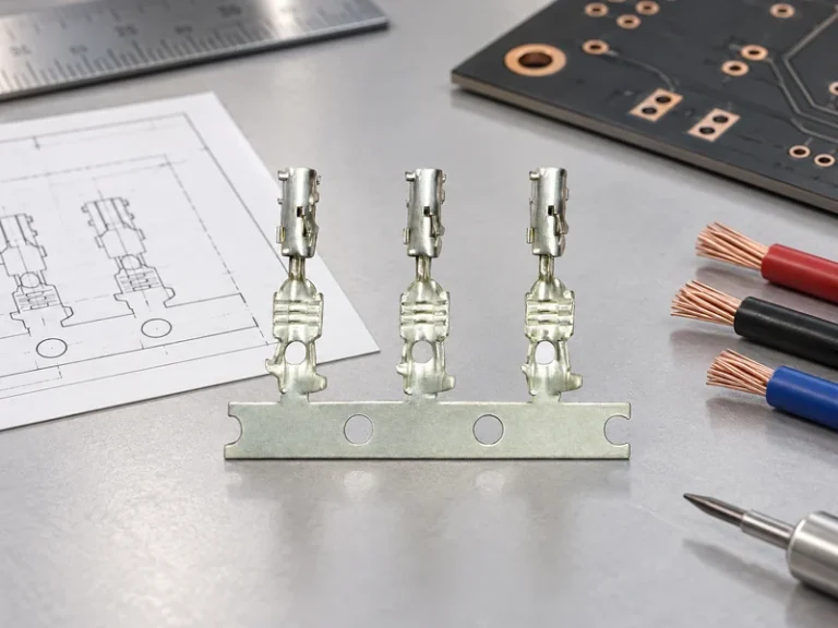
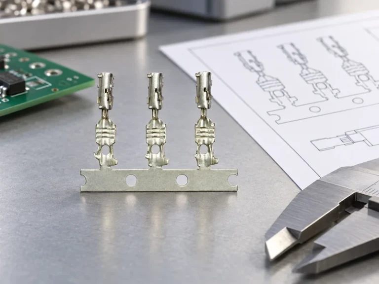
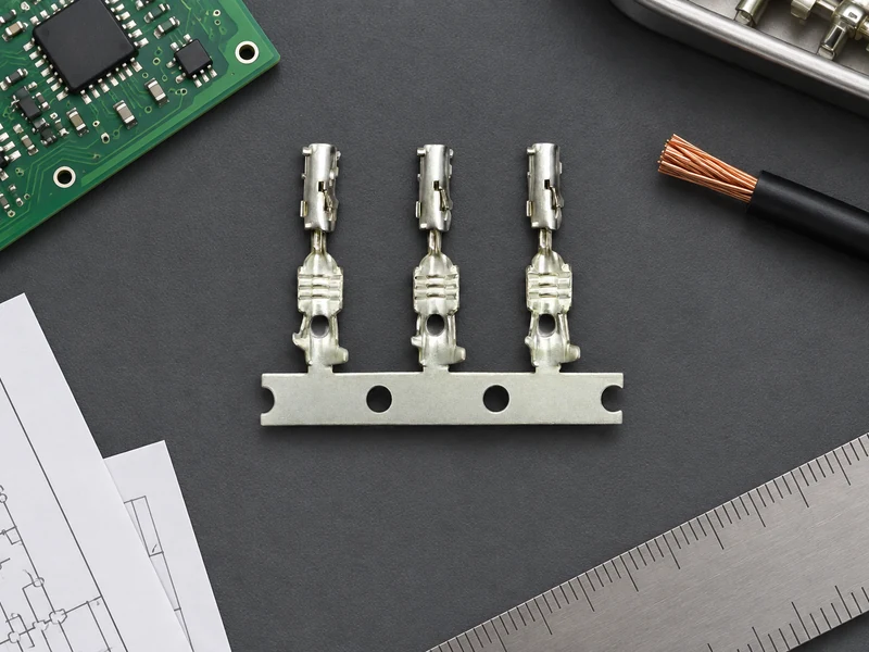
First classify the connection path. A wire-to-board architecture brings a cable or harness to the PCB and must control the header, housing or receptacle, crimp terminal, wire range, tooling and footprint as one mating system. A board-to-board architecture joins two PCBs, so stack height, coplanarity, alignment tolerance and insertion travel become primary constraints. A removable service interface may use either architecture, but it also needs an accessible release method, polarization, a defined replacement mate and a realistic mating-cycle requirement. These architectures can share the same nominal pitch while creating very different assembly and maintenance risks.
Choose the architecture against the product’s replacement boundary. If technicians replace a harness but not the PCB, place the separable interface where the mating half and latch remain accessible. If two boards are joined only during factory assembly, service-cycle features may consume space without helping the intended process. If a daughterboard is replaceable, guides, standoffs or other mechanical datums should align the boards before the contacts carry insertion load. These are system-level decision rules, not universal product claims; confirm the chosen family’s drawings, approved mates and test conditions.
Use open headers only when the assembly controls alignment and accidental contact is acceptable. Use a shroud, key and latch when operators need positive orientation or retention. A right-angle design may improve cable routing but moves the mating force parallel to the PCB; an SMT design saves drilled holes yet may need mechanical hold-downs if users pull on the harness.
| Type | Layout advantage | Control needed | Procurement question |
|---|---|---|---|
| Vertical through-hole | Direct top entry and mechanical anchoring | Insertion height and solder process | What is the recommended hole pattern? |
| Right-angle through-hole | Board-edge cable exit | Edge datum and enclosure clearance | Is the tail geometry drawing-controlled? |
| Vertical SMT | Single-side assembly flow | Pad layout, coplanarity and peel load | Are hold-downs required? |
| Shrouded/keyed | Guided and polarized mating | Matching housing and key code | Which exact parts are approved mates? |
| Board-to-board | Compact module stacking | Stack height and alignment tolerance | What misalignment can the pair accept? |
Evaluate pin count and electrical loading together
Pin count begins with active circuits but should also consider grounds, reserved positions, coding and service strategy. Adding positions can support future variants, yet it increases width and creates more opportunities for partial mating. Build a pin-assignment table that identifies power, return, signals and unused contacts; do not allow “spare” contacts to float into production without an agreed rule.
For circuit board wire connectors, current must be reviewed at the loaded-connector level. Do not multiply a catalog’s per-contact current value by every occupied circuit and call the result connector capacity. That value may come from one energized contact, a particular conductor size, a specified ambient or another family-specific test arrangement. In a fully loaded housing, adjacent powered contacts create mutual heating, while PCB copper, wire gauge, termination quality and enclosure airflow may become the limiting elements. IEC 60512 offers relevant electrical test methods, including contact resistance and current-carrying evaluations. Ask for the exact sample arrangement, energized-position pattern, ambient condition, temperature-rise limit and acceptance criteria behind supplier data, then test the worst credible loading configuration.
A credible pin connection specification also separates nominal voltage from insulation coordination. Clearance, creepage, contamination and altitude affect the design. IPC-2221 provides general PCB design guidance, but the final geometry must reflect the connector drawing, destination rules and end-product safety assessment.
Make the board layout follow the mating and service path
Place the connector with the full mating envelope visible in the mechanical model. Confirm whether the plug approaches vertically or horizontally after nearby boards and enclosure panels are installed. Record any connector overhang beyond the PCB edge because it affects board support, guides, handling and enclosure clearance. Define a mechanical keep-out for the mating housing, latch sweep and extraction tool rather than reserving only the header outline. Include cable-exit direction, minimum bend space, finger or tool access and the clearance required to release the latch without levering against the PCB. Keep tall components away from the insertion path and prevent the harness from transferring constant side load into solder joints. A serviceable interface is not serviceable if a technician must remove another assembly or bend the board to reach its lock.
A circuit board connector near a board edge may simplify routing, but the designer still needs a datum scheme: PCB edge to connector centerline, connector seating plane and permitted angular error. For through-hole parts, use the supplier’s finished-hole and land recommendations. For SMT parts, review pad geometry and board support during mating. Do not reuse a footprint merely because another part shares the same pitch.
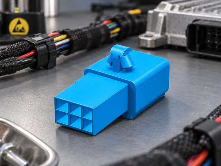
Automotive housings show why polarization and retention deserve early attention. CNSJ’s Polarized Automotive Receptacle is an adjacent application reference, not a PCB-header substitute. Its product category reinforces the system question: how will the assembly prevent a plausible human mating error?
| Design dimension | Minimum evidence | Prototype check | Release criterion |
|---|---|---|---|
| Pitch and pattern | Controlled mechanical drawing | First-article measurement | Footprint matches drawing revision |
| Mating envelope | 3D model plus keep-out | Mate/unmate in enclosure | No interference or board flex |
| Electrical loading | Test report for comparable loading | Temperature-rise trial | Within project limit with margin |
| Retention | Latch/withdrawal-force data | Harness pull direction check | No unintended release |
| Assembly | Footprint and process guidance | Pilot solder inspection | Meets the chosen workmanship class |
| Service life | Mating-cycle test conditions | Cycle representative samples | Resistance and mechanics remain acceptable |
Use environmental and lifecycle evidence before sourcing
Many board-level headers are intended for protected interiors and should not be assumed sealed. If the assembly faces water, dust or chemicals, define the enclosure strategy and verify whether sealing applies to the connector, the mated interface or the final product. An IP code describes enclosure protection under IEC 60529 conditions; it does not automatically prove vibration life or chemical resistance.
Vibration validation should reproduce mounting, harness mass and excitation direction. Mechanical operation tests in IEC 60512 can help structure mating-cycle verification, while the application must set an appropriate cycle count and end criteria. Track contact resistance, retention and physical damage before and after exposure. A “passed” statement without configuration and criteria is not procurement-grade evidence.
Workmanship and compliance deserve separate files. IPC-A-610 addresses electronic assembly acceptance, and IPC/WHMA-A-620 addresses cable and wire-harness assemblies. EU RoHS and REACH documentation concerns substances; those declarations do not prove electrical performance. Match every claim to the exact part number and manufacturing revision.
What the validation package should contain before sourcing
- Freeze functional circuits, pin assignment and the desired spare-position policy.
- Define straight/right-angle, SMT/through-hole, shrouding, polarization and latch needs.
- Obtain approved mating-part numbers, drawings, footprint data and tooling instructions.
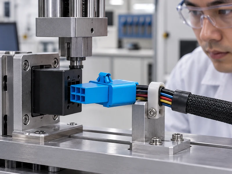
- Run a production-intent build with actual wire, crimp contacts, PCB finish and enclosure.
- Record the test configuration, acceptance limits, BOM revision and supplier change-control terms.
CNSJ Connector’s published range is automotive-connector-focused. Pages such as its Compact Automotive Coupler and the Battery Connector Terminal guide can inform adjacent decisions about packaging and terminated contacts; they do not confirm that an equivalent pin-header product is offered.
Compare suppliers with the same evidence set
Send every bidder the same drawing, load table and environmental profile. Require a deviation list so that silence is not interpreted as compliance. For circuit board wire connectors, compare the complete cost of housings, terminals, tooling, packaging and inspection—not the header alone. Record whether alternates require another footprint or crimp qualification.
The approved pin connection should also have a continuity strategy. Buyers need lead-time expectations, lifecycle status, traceability and product-change notification terms. A second source is useful only if its mating geometry and performance have been independently validated. Likewise, each circuit board connector option should arrive with a revision-controlled evidence pack that engineering and quality teams can audit later.
Pin connector FAQs for layout and loading decisions
How do you choose pin count for a pin header connector?
Count required power, return and signal circuits, then add only justified grounds, coding positions or future reserves. Check connector width, partial-mating risk and routing space before adding spare contacts. Document every position in the interface-control drawing.
What is the difference between through-hole and SMT pin header connectors?
Through-hole contacts pass through drilled PCB holes and can provide strong mechanical anchoring, while SMT contacts solder to surface pads and support surface-mount process flows. The better option depends on board construction, mating loads, available area and assembly capability; neither technology is universally stronger.
How does pin connector affect board layout?
A pin connector determines the footprint, keep-outs, insertion direction, cable bend space and service access. It also influences copper routing and mechanical support. Place it from a complete mated model, not from the header outline alone.
What current rating should a pin header connector have?
The rating should exceed the application load under the actual ambient, number of energized contacts, conductor size and acceptable temperature rise. Use supplier test evidence for the exact family, then validate the worst credible configuration rather than applying a generic per-pin number.
Which Sources Support Pin Connector Architecture, Layout and Validation Decisions?
- Phoenix Contact: PCB connector architectures and selection fields
- IEC 60512-1: General connector test and measurement guidance
- IEC 60529 enclosure protection (IP Code)
- IPC-2221B, Generic Standard on Printed Board Design
- IPC-A-610, Acceptability of Electronic Assemblies
- European Commission: RoHS Directive
A connector fits the product only when its electrical, mechanical and human interfaces fit at the same time.
Buyer CTA: Review the automotive connector range, then send CNSJ Connector your pin map, envelope drawing, mating direction, wire range, PCB process, environment and annual demand. Request a written compatibility response and supporting documents for any proposed solution; treat automotive catalog examples as adjacent references until a specific board-level product is confirmed.