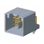


Choosing a pcb pin header is a board-interface decision, not a cosmetic part-number lookup. The correct choice must fit the mating housing, pitch, row geometry, orientation, termination process, keep-out and inspection plan. This guide gives buyers and design engineers a practical sequence for selecting a pin header PCB component while keeping claims bounded by the supplier drawing.
In brief: freeze the mating connector first, then verify pitch, positions, contact length, body height, terminal finish, mounting method and the manufacturer’s land pattern. A “pin header plug” may refer to a separate housing or to a complete cable assembly, so request the exact mating part rather than relying on a generic search label.
What is a PCB pin header?
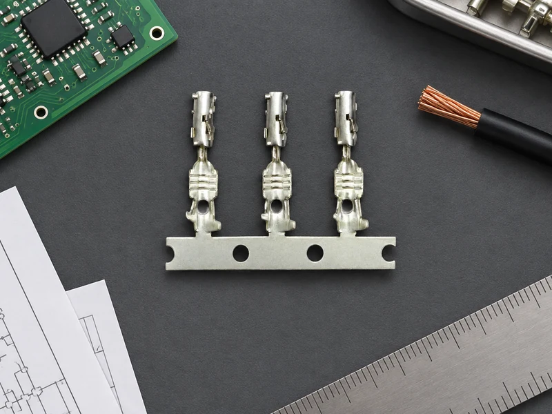
Record the number of rows and positions, pitch, contact tail style, insulator height, mating length, orientation, shroud or key, board-lock feature and packaging. If the assembly uses a cable housing, list that housing beside the board part. Bare posts and shrouded headers can share a pitch while having different mating and polarization behavior.
Use pin header pcb as a board-layout search term, not proof of interchangeability. The released drawing should identify pin one, datum edges, plated-hole or SMT dimensions, component-side orientation and any no-copper or courtyard requirements. IPC-2221 is a useful generic board-design reference, but it does not replace the component drawing.
| Specification block | Buyer evidence | Design consequence |
|---|---|---|
| Pitch and positions | Supplier dimensional drawing | Controls hole or pad pattern and mating alignment |
| Orientation | Vertical, right-angle or custom drawing | Controls cable exit and enclosure clearance |
| Termination | Through-hole or SMT process recommendation | Controls solder profile, tooling and inspection |
| Shroud and key | Mating housing drawing | Controls polarization and error prevention |
What is the standard pitch of a pin header?
Pitch sets the nominal center spacing, but the footprint also depends on row spacing, finished-hole diameter, pad shape, tail length and insertion depth. A right-angle header can fit a board edge yet fail the enclosure because the cable sweeps through a neighboring component. A vertical part can clear the housing but exceed the service height above the board.
Import the approved land pattern into the CAD review and compare it with the real mating housing. Keep a visible pin-one reference and check solder-side access. For dense boards, model probe access, rework clearance and the cable bend rather than assuming that a compact outline is automatically serviceable.
How do you choose the right pin header connector for a PCB?
Choose a shroud when the mating housing needs polarization or when accidental offset is a credible assembly risk. Choose an unshrouded row when the application intentionally uses a simple contact interface and the assembly process has another way to control orientation. Board locks can assist placement, but their presence and geometry must be verified from the drawing.
The mating housing is part of the specification. A pin header plug from one family may not fit a visually similar row from another family because contact length, insulator wall and latch geometry differ. Request samples of both halves and record the approved combination in the BOM.
| Application condition | Preferred review | Inspection evidence |
|---|---|---|
| Frequent unplugging | Housing latch and contact retention review | Controlled mating/unmating observation |
| Board-edge installation | Right-angle body and cable sweep review | Enclosure fit sample |
| Automated placement | Packaging, pick point and board locks | First-article placement record |
| Dense inspection area | Probe and camera line-of-sight review | AOI and rework access check |
How do you check a PCB pin header footprint and solder joint?
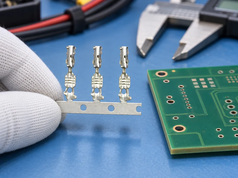
Verify the received marking and lot, compare pitch and body dimensions, confirm the mating housing, and inspect solder joints against the approved workmanship standard. If the process uses a wire terminal crimping tool elsewhere in the harness, keep that operation separate from the PCB header acceptance criteria; one tool does not prove the board interface.
Use IEC 60512 for agreed connector test methods, IPC-2221 for board-design context and IPC-A-610 for assembly acceptability. Buyers can also review the CNSJ connector knowledge base, automotive connector products, contact page and company information when building a supplier shortlist.
A useful CAD review begins with the board datum and the mating datum. Lock the first row, pin one and the board edge before copying the pattern to another sheet. Then check solder mask expansion, paste coverage for SMT parts, finished-hole assumptions for through-hole parts and the effect of panel rails. These checks keep a nominal pcb pin header footprint from becoming a production-specific surprise.
Also review how the connector arrives at the line. Tape-and-reel, tube and tray packaging create different pick-and-place constraints. If a header has a temporary cap or protective film, define when it is removed and where the part is inspected. Packaging is part of the process capability, not an afterthought to the electrical drawing.
For low-volume prototypes, technicians may mate a cable by hand; for high-volume builds, a guided housing and fixture can control insertion. The approved work instruction should name the mating half, show the keying feature and state what a fully seated condition looks like. This makes the same pin header pcb decision repeatable across shifts and suppliers.
Keep alternates under engineering change control. A substitute may share pitch but change contact length, plastic height or solder-tail geometry. Before approval, run the same enclosure, mating, solder and inspection checks used for the original. That evidence is more reliable than a supplier statement that two headers are “equivalent.”
Thermal and mechanical context should be included in the footprint review. A header beside a heat sink can experience a different assembly sequence from one in an open board area. Confirm that the selected plastic body, contact finish and cable exit are suitable for the documented process environment, and keep any temperature or material statements tied to a controlled supplier document.
For multi-board systems, align the datum strategy across every board that uses the same family. A connector that is offset by one pitch can still appear to mate during a loose bench check but fail when boards are fixed in their final guides. Use a fixture or enclosure sample to verify alignment at the stack-up limits, not just at nominal CAD dimensions.
Quality teams should be able to identify a wrong header without an electrical test. A pin-one mark, shroud, key, board-lock pattern, body height and terminal finish provide useful visual evidence. Add those attributes to the receiving checklist and take one reference photograph from the same angle used on the production line.
When all evidence is ready, release the pin header plug and board component as a matched pair in the purchasing specification. Include approved alternates only after the same mating, footprint, assembly and inspection reviews are complete. This approach makes the selected pcb pin header repeatable across suppliers and production sites.
A design-for-assembly review should follow the connector through the entire factory route. Confirm that placement equipment can reach the part, that the board remains supported during insertion, and that soldering does not leave the body tilted. After soldering, inspectors need a clear view of the joints and the mating face. If rework is possible, define the removal method and protect adjacent plastic parts from unintended heat.
For purchasing, attach the controlled drawing to the inquiry and ask suppliers to mark every proposed deviation. This prevents an alternate material, plating or packaging change from being hidden behind a matching headline description. Sample approval should use the intended mating housing and enclosure rather than a loose desktop connection. Record the final part number, drawing revision, approved source and inspection evidence before volume ordering.
PCB pin header FAQs
Is a pin header PCB footprint universal?
No. Pitch, row spacing, tail geometry and approved mating parts vary by series.
Does a shroud always prevent reverse insertion?
Only when the mating housing and keying features are designed as a matched pair.
Can a right-angle header use the same land pattern as a vertical header?
Not automatically. Confirm tail geometry, body datum and cable clearance with the supplier drawing.
What should be in the first-article report?
Part identity, dimensions, pin-one orientation, mating result, solder or press-fit evidence and any agreed test records.
Send the board outline, mating housing, pitch, orientation and assembly process to CNSJ for a documented pcb pin header review and sourcing recommendation.
What to confirm before ordering a PCB pin header
A robust pcb pin header selection links the board footprint to the approved mating housing, assembly process, enclosure and inspection plan. Freeze those references before purchasing, validate the first article in its real mechanical stack-up and review every alternate against the same evidence.